AR
C
HIVE INF
O
RMATI
O
N
A
RCHIVE INFORMATION
2
RF Device Data
Freescale Semiconductor
MRF18085ALR3 MRF18085ALSR3
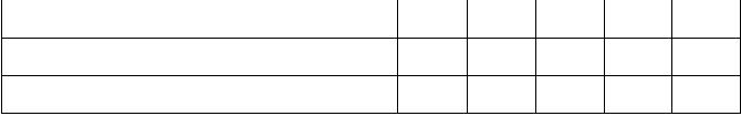
Table 4. Electrical Characteristics
(TC
=25°C unless otherwise noted)
Characteristic
Symbol
Min
Typ
Max
Unit
Off Characteristics
Drain--Source Breakdown Voltage
(VGS
=0Vdc,ID
= 100
μAdc)
V(BR)DSS
65
?
?
Vdc
Zero Gate Voltage Drain Current
(VDS
=26Vdc,VGS
=0Vdc)
IDSS
?
?
10
μAdc
Gate--Source Leakage Current
(VGS
=5Vdc,VDS
=0Vdc)
IGSS
?
?
1
μAdc
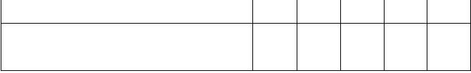
On Characteristics
Gate Threshold Voltage
(VDS
=10Vdc,ID
= 200
μAdc)
VGS(th)
2
?
4
Vdc
Gate Quiescent Voltage
(VDS
=26Vdc,ID
= 600 mAdc)
VGS(Q)
2.5
3.9
4.5
Vdc
Drain--Source On--Voltage
(VGS
=10Vdc,ID
=2Adc)
VDS(on)
?
0.15
?
Vdc
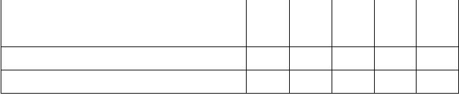
Dynamic Characteristics
Reverse Transfer Capacitance
(1)
(VDS
=26Vdc,VGS
=0,f=1MHz)
Crss
?
3.6
?
pF
Functional Tests
(In Freescale Test Fixture, 50 ohm system)
Common--Source Amplifier Power Gain @ 85 W
(2)
(VDD
=26Vdc,IDQ
= 800 mA, f = 1805 -- 1880 MHz)
Gps
13.5
15
?
dB
Drain Efficiency @ 85 W
(2)
(VDD
=26Vdc,IDQ
= 800 mA, f = 1805 -- 1880 MHz)
η
48
52
?
%
Input Return Loss @ 85 W
(2)
(VDD
=26Vdc,IDQ
= 800 mA, f = 1805 -- 1880 MHz)
IRL
?
-- 1 2
-- 9
dB
Power Output, 1 dB Compression Point
(VDD
=26Vdc,IDQ
= 800 mA, f = 1805 -- 1880 MHz)
P1dB
83
90
?
Watts
1. Part is internally matched both on input and output.
2. To meet application requirements, Freescale test fixtures have been designed to cover the full GSM1800 band, ensuring
batch--to--batch consistency.


发布紧急采购,3分钟左右您将得到回复。
相关PDF资料
MRF18090AR3
IC MOSFET RF N-CHAN NI-880
MRF19030LSR5
IC MOSFET RF N-CHAN NI-400S
MRF19045LR3
IC MOSFET RF N-CHAN NI-400
MRF19085LR3
IC MOSFET RF N-CHAN NI-780
MRF19090SR3
IC MOSFET RF N-CHAN NI-880S
MRF19125R5
IC MOSFET RF N-CHAN NI-880
MRF21010LSR1
IC MOSFET RF N-CHAN NI-360S
MRF21030LR3
IC MOSFET RF N-CHAN NI-400
相关代理商/技术参数
MRF18085AR3
制造商:MOTOROLA 制造商全称:Motorola, Inc 功能描述:RF Power Field Effect Transistors
MRF18085AR5
制造商:Rochester Electronics LLC 功能描述: 制造商:Freescale Semiconductor 功能描述:
MRF18085B
制造商:Motorola Inc 功能描述:
MRF18085BLR3
功能描述:MOSFET N-CHAN 85W 26V NI-78O RoHS:是 类别:分离式半导体产品 >> RF FET 系列:- 产品目录绘图:MOSFET SOT-23-3 Pkg 标准包装:3,000 系列:- 晶体管类型:N 通道 JFET 频率:- 增益:- 电压 - 测试:- 额定电流:30mA 噪音数据:- 电流 - 测试:- 功率 - 输出:- 电压 - 额定:25V 封装/外壳:TO-236-3,SC-59,SOT-23-3 供应商设备封装:SOT-23-3(TO-236) 包装:带卷 (TR) 产品目录页面:1558 (CN2011-ZH PDF) 其它名称:MMBFJ309LT1GOSMMBFJ309LT1GOS-NDMMBFJ309LT1GOSTR
MRF18085BLSR3
制造商:Rochester Electronics LLC 功能描述: 制造商:Freescale Semiconductor 功能描述:
MRF18085BR3
制造商:MOTOROLA 制造商全称:Motorola, Inc 功能描述:RF Power Field Effect Transistors
MRF18090A
制造商:MOTOROLA 制造商全称:Motorola, Inc 功能描述:1.80 - 1.88 GHz, 90 W, 26 V LATERAL N-CHANNEL RF POWER MOSFETS
MRF18090AR3
功能描述:IC MOSFET RF N-CHAN NI-880 RoHS:是 类别:分离式半导体产品 >> RF FET 系列:- 产品目录绘图:MOSFET SOT-23-3 Pkg 标准包装:3,000 系列:- 晶体管类型:N 通道 JFET 频率:- 增益:- 电压 - 测试:- 额定电流:30mA 噪音数据:- 电流 - 测试:- 功率 - 输出:- 电压 - 额定:25V 封装/外壳:TO-236-3,SC-59,SOT-23-3 供应商设备封装:SOT-23-3(TO-236) 包装:带卷 (TR) 产品目录页面:1558 (CN2011-ZH PDF) 其它名称:MMBFJ309LT1GOSMMBFJ309LT1GOS-NDMMBFJ309LT1GOSTR